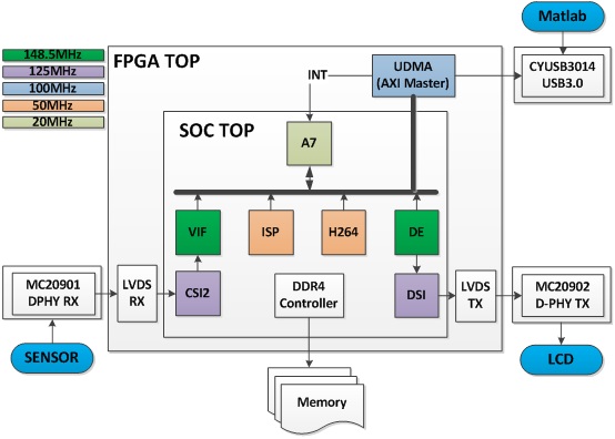
The FPGA verification system consists of image sensor, LCD display and PC running ISP tools. With this system, verification engineer can get real time image data from ISP or H264 which will improve work efficiency.
Outline
- USB3.0 board
- DPHY RX/TX Board
- USB/FPGA Protocol
- UDMA Structure
- LVDS RX/TX Structure
System structure diagram is as following and the SOC is targeted at image signal processing and encoding with real-time video source.
The following two daughter cards need to be made:
- USB3.0 board is used for PC to access memories and registers in SOC
- DPHY RX/TX board is used for transfer DPHY signal to LVDS level
USB3.0 Board
USB3.0 board is responsible for communication with PC software. The whole FPGA system can be see as a memory space and the software can access all address in FPGA and SOC.
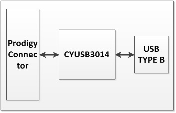
Componets
- CYUSB3014: USB3.0 chip which provide PHY and controller
- USB TypeB (or MicroB) connector
- Prodigy connector: connect to S2C UV440 FPGA platform
Feature
- USB driver
- USB print class: no need to install driver
- WinUSB driver: recommended for applications
- FIFO interface of CYUSB3014 can provide 3200Mbps throughput
- PCLK pin shall connect to GCLK pin of FPGA
- PCB design guidelines
- Minimize the trace length of USB lines (<3 inches)
- The polarity can be swapped on the differential pairs
- Tie the R_USB2 pin to ground through 6.04kΩ resistor. Tie the R_USB3 pin to ground through 200Ω resistor
- USB 3.0 traces require additional AC coupling capacitors (0.1 uF) places on the SS_TX lines. Place these capacitors symmetrically and close to FX3 device
- Keep the USB signal line impedance at 90Ω differential
- Fill the space between the two differential pairs with ground
- Keep the crystal trace as short as possible (<2 cm)
- Use split planes on the power layer for different power domains
- Power trace width should be > 25 mils to reduce inductance
- Keep power traces as short as possible and away from high speed data and clock lines
- Do not place vias in a trace
- Avoid stubs on all USB lines. The testing probe should not extend out of the trace
- On the USB signal lines, use rounded bends if necessary
- Do not place differential pairs close to other high-speed signals to avoid cross talk
DPHY RX/TX Board
DPHY RX board is used to receive data from image sensors complient with MIPI specification. DPHY TX board can connect to typical touch screen LCD to preview.
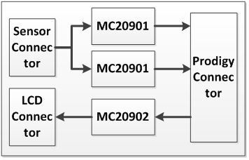
Componets
- MC20901: transfer MIPI signal level to LVDS and LVCMOS for FPGA IO
- MC20902: transfer LVDS and LVCMOS signal into MIPI signal level
- Prodigy connector: connect to S2C UV440 FPGA platform
- LCD connector: connect to DSI LCD
- Sensor connector: connect to MIPI sensors
Feature
- MC20901/MC20902
- Accept LVDS (DPHY HS) signal up to 2.5Gbps
- Accept LVCMOS (DPHY LPDT) signal up to 20Mbps
- PCB design guidelines
- Match the length of all differential traces (data and clock)
- When making turns with differential traces, balance the number of left and right turns
- Do not route traces into 90゜or 180゜turns
- Spread traces after routing over the available space of the PCB to minimize crosstalk
- Use dedicated and separate planes for power and ground
- Run high-speed signals on the outer layers of the PCB
- Provide enough space between pairs of differential traces and enough space between signal traces and nearby ground planes on the same layer
- Do not place vias in a trace
USB/FPGA Protocol
The software should obey this protocol when it get image through USB3.0. Each packet sent from PC has a header and payload. The header has 12 bytes and the maximum payload size should less than 2M bytes.
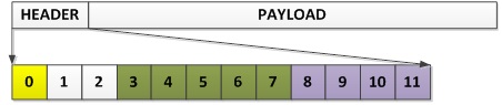
Byte0: indicates write or read operation.
Byte1 ~ Byte2: reserved.
Byte3 ~ Byte7: operation address.
Byte8 ~ Byte9: total length of Header and Payload.
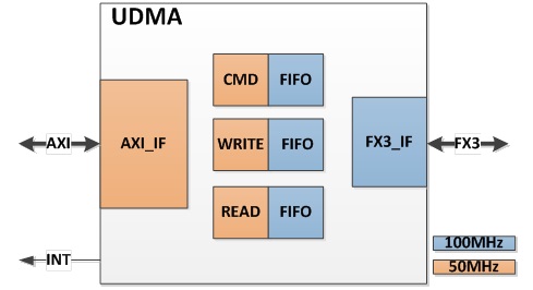
UDMA Structure
UDMA module is responsible for reading/writing data with FPGA. The AXI_IF will connect to NOC which runs at 50MHz and FX3_IF will connect to CYUSB3014 running at 100MHz.
There are three FIFOs to synchronize data and command between AXI and FX3. Since FPGA has large BRAM resources, the CMD_FIFO is 256 bytes; the WRITE_FIFO is 2K bytes and the READ_FIFO is 32K bytes.
The FX3_IF actually is a slave FIFO controller and the input/output delay for data and control should be constraint carefully.
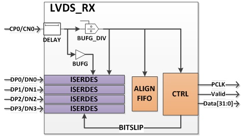
LVDS RX/TX Structure
LVDS_RX module is responsible for receiving data from MC20901. All data lanes will be decode by ISERDES. For clock lane, firstly, 90 degree phase delay is necessary for double data rate transactions; secondly, BUFG_DIV will divide bit clock into byte clock for ISERDES. ALIGN_FIFO module will search “SYNC CODE” (00011101) of DPHY. CTRL module will generate “BITSLIP” signal to adjust ISERDES according to alignment.
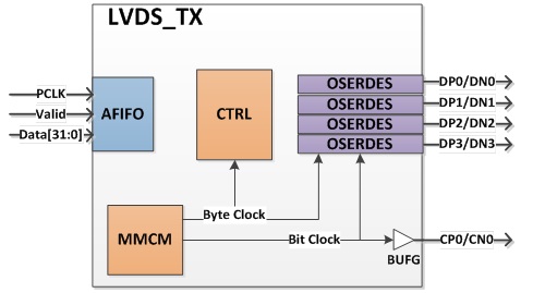
LVDS_TX module is responsible for transmitting data to MC20902. AFIFO module will synchronize the data from DSI controller. MMCM will generate bit clock and byte clock. OSERDES will serialize data into differential high speed signals.